Perspectives on BICS9 3D-NAND: Sandisk could beat Samsung V10 with memory density 4 comments
Image: Sanisk
Sandisk is working with Koxia on the next generation of NAND-Flash. BICS8 follows BICS9 and the number of layers increases from 218 to over 300. At Sandisk’s investor day, there was a little view and lesson why Bics Flash is the best in the industry.
BICS9 with more density and more performance
In terms of memory density, BICS9 would increase by around 59% compared to BICS8. For a long time, this does not mean that costs decrease to the same extent. The additional locations in turn mean more necessary work steps with associated costs.
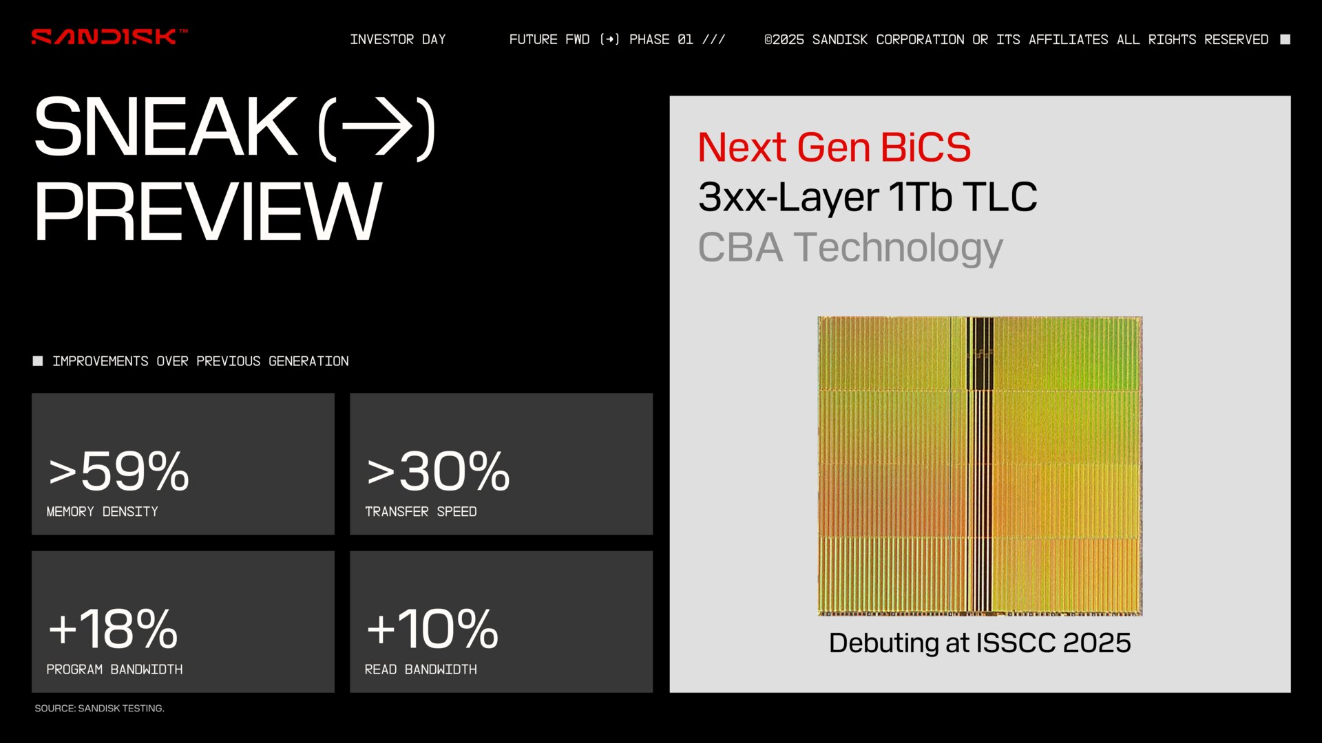 Sandisk provides a small overview of BICS9 (Image: Sandisk)
Based on the 18.3 GBIT/mm², which is officially mentioned as the memory density for BICS8 (TLC), an increase would mean 59% of the memory density of a whopping 29.1 Gbit/mm² for BICS9 (TLC). This would also make Samsungs high performance TLC-NAND layer class 4xx. For now, however, this is just an estimate. For ISSCC 2025 in the coming week, Kioxia and Sandisk want to reveal more. Samsungs V10-Nand is also on the plan.
The “transfer speed” should be over 30% higher, which is supposed to be visible. Sandisk partner Kioxia wants to introduce TLC-NAND with an I/O speed of 4.8 GBIT/s on the ISSCC 2025 TLC-NAND. However, this would be a 50% increase from 3.2 GBIT/S at BICS8.
30.2A 3B/cell 1TB 3D Flash Memory with 29% Energy Efficient Read Operation and 4.8GB/s Low Termination IOS Low Application.
Kioxia, from the ISSCC 2025 program
There is also an 18% increase in write throughput (program width) and a 10% increased read rate (read bandwidth).
Sandisk not participating in diaper race
From the point of view of Sandisk and kioxie, adding more levels (layer) in 3D-NAND is a simple, but not very effective and not very economical measure to further increase the bit density. The joint venture of Koxia and Sandisk with 218 layers is currently clearly behind competitors such as Samsung (286 layers) and Micron (276 layers). But with bit-per-layer density, Sandisk / Koxia is a leader and thus achieves high surface density with only 218 layers.
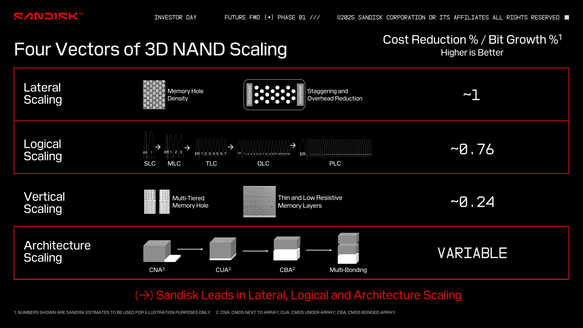 Which measures for scaling 3D-NAND are most effective from Sandisk’s point of view (Image: Sandisk)
The manufacturer also sees its own BICS8 better positioned in performance and energy efficiency than current competition. The comparison is late without concrete values or naming the selected competitor.
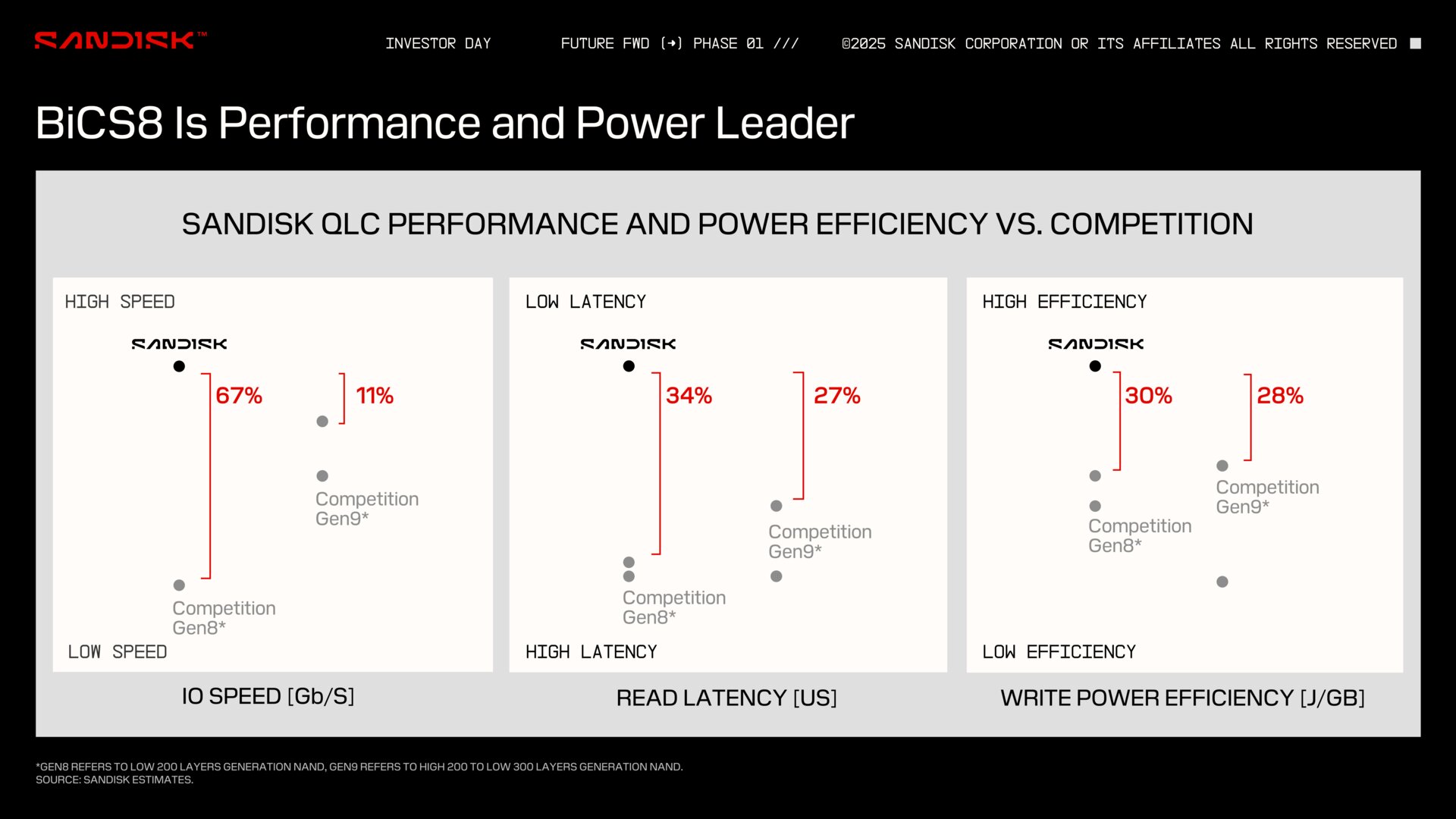 Sandisk compares BICS8 with a competitor (Image: Sandisk)
For the first time, Koxia and Sanisk at BICS8 relied on a manufacturing process with Waferbonden, as already demonstrated by Chinese newcomer YMTC. Levels with memory cells are made on a separate level and logic on another. The two wafers are finally connected, the procedure is called “direct-board CMOS”, for short CBA, in Sandisk and Kioxia. CBA must also be used in BICS9.
Topics: 3D-NAND Flash Memory ISSSCC 2025 Koxia SANDISK STORAGE WESTERNE WESTER

Alice guides you through the best storage solutions, from ultra-fast SSDs to secure cloud options.