ISSCC 2025: Samsung prepares 4xx Layer V10 TLC NAND with 5.6 Gb/s 7 comments

Image: Samsung
The International Solid-State Circuits Conference, or ISSCC 2025 for short, begins in February. Technical details on new semiconductor products can be expected here. The same goes for next-generation 3D NAND. What Samsung, SK Hynix and Kioxia are planning seems impressive to say the least.
Samsung TLC-NAND 4xx layer
While this year the focus has been on QLC-NAND with 28.5 Gbit/mm² (see cover photo), which offers the highest areal density of 3D NAND to date, Samsung aims to achieve this with a future generation with TLC and 3 bits per cell.
“28Gb/mm² 4XX-Layer 1TB 3b/cell WF-Bonding 3D-NAND Flash with 5.6Gb/s/pin IOs” is a session planned by Samsung at ISSCC 2025. TLC -NAND with “4xx”, or over 400 layers, should have almost as much storage capacity per area at 28 Gbit/mm² QLC NAND 286 layers of the V9 generation, which began mass production in September.
Also noteworthy is the fast 5.6 Gbps per pin NAND interface. The fastest NAND chips to date in this regard are 3.6 Gbps.
Samsung has long been a leader in 3D NAND, but has fallen behind in recent years and now needs to catch up. The fact that Samsung is using wafer bonding in production for the first time with the 4xx NAND layer has long since happened to its competitors. YMTC had already trusted it with its “XTacking” architecture, Kioxia and Western Digital recently followed suit with their BiCS8 flash.
Wafer bonding describes a manufacturing step in which two silicon wafers are bonded together over the entire surface. In the case of 3D NAND, the chip logic (I/O) and the memory area are initially manufactured separately on separate wafers and then combined to form a memory chip. Even if two wafers are required, the overall costs should not increase, as the storage density can be significantly increased, making it worthwhile.
Samsung to skip the 3xx layer
There have already been rumors that Samsung will jump directly from its 286-layer NAND of the V9 generation to over 400 layers, skipping the 3xx layers. There was talk of 430 layers on the Samsung V10. The planned presentation at ISSCC now further supports this assumption.
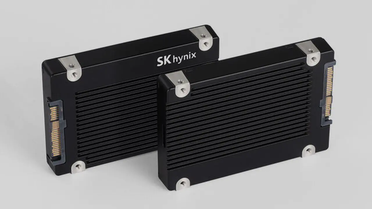
SK Hynix recently launched its 321-layer TLC NAND into mass production. 2-Tbit-QLC with 321 Layern by SK Hynix
Kioxia and Western Digital currently offer the highest storage capacity (not density) in 3D NAND with the BiCS8-QLC-NAND, which has 2 Tbits per chip. SK Hynix also plans to provide this storage capacity soon with its QLC variant of the 321-layer NAND. The QLC-NAND is also expected to achieve a write rate of 75 MB/s at the chip level. This is very fast for QLC storage. The 60 MB/s of Kioxia’s BiCS6 QLC was already considered fast two years ago.
321-layer, 2 TB, 4-bit/cell 3D-NAND-Flash with a program throughput of 75 MB/s
SK Hynix for ISSCC 2025
Efficient TLC at Kioxia
At Kioxia and Western Digital, the focus is once again on energy efficiency. The next ISSCC session is titled “A 1TB, 3b/cell 3D Flash Memory with 29% Improved Energy Efficiency Read Operation and 4.8% Low Termination and Isolated I/O GB/s. » So this is a new TLC memory with 3 bits per cell and 1 Tbit per chip, which is supposed to work 29% more efficiently when reading. It remains to be seen exactly what is being compared here.
Topics: Kioxia Samsung SK Hynix Storage TLC 3D NAND flash memory Western Digital Source: ISSCC

Alice guides you through the best storage solutions, from ultra-fast SSDs to secure cloud options.