Nintendo Switch 2: Detailed PCB Photos and Shots Published

Nintendo Switch 2: Detailed PCB Photos and Shots Published
Image: Kurnal
The first detailed shots of a stock Switch-2 PCB and the integrated SOC plans have come from China. After years of rumors, it has been confirmed that it is in fact the Nvidia Tegra T239 with an Ampere architecture manufactured at Samsung in 8nm. The Nintendo Switch 2 will be released on June 5, 2025.
PCB records confirm the four-year-old leak
This also applies to Asia, so the photographed boards are not from a retailer. Instead, the components come from a second-hand marketplace, roughly comparable to eBay. In fact, it is not uncommon for hardware or early samples to reach the public prematurely through these channels. In any case, both PCBs of the Switch 2 are already in stock, and the SOC with a processor and graphics unit, as well as 12 GB of GDDR5X memory, are also available.
Nintendo already mentioned an Nvidia chip at the beginning of April during the presentation of the handheld console; however, there was no official architecture or model name yet. Now it’s clear: it’s actually the Tegra T239 with Ampere architecture, which the rumor mill has been referring to as a Switch 2 chip since June 2021. It’s extremely remarkable that such information was correctly stabbed four years before the release of the relevant product, and anything but usual.
A die-shot shows the ARM CPU and Ampere GPU
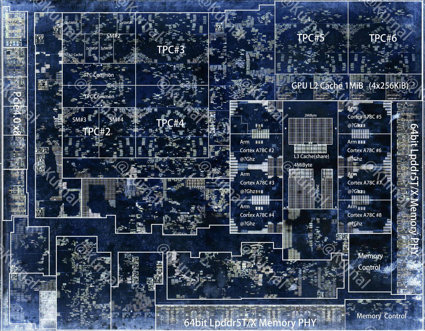 Nvidia T239 Nintendo Switch 2 Photo Shot (Image: Kurnal)
The only 128-bit memory interface can be found with the memory controller at the bottom right. While the RTX 3050 in question also doesn’t return to 128-bit, 14 Gbps are attached to fast GDDR6 modules. The GDDR5X memory of the Switch 2 is expected to climb considerably lower, offering a total of around 100 GB/s.
A major advantage of the T239 with AMPERE architecture over older Switch models is the integrated tensor cores in the SMS and thus DLSS support. Nintendo previously confirmed that it wanted to use the upsampling feature, but ultimately passed it on to game developers. DLSS frame generation is off the table with an Ampere chip. The PCB and TEGRA SOC video, also available with an English setting, also makes initial considerations and assumptions about hardware performance and draws comparisons with notebook graphics cards. However, such comparative positions are absolutely effective, games are generally dedicated to games have produced millions of consoles and all configured to identification.
Nintendo Switch 2, OLED Switch, and Switch specifications in the Switch 2 comparison: OLED Switch Dimensions: 272 × 116 × 13.9 mm (with Joy-Con)
(thickest point: 30.7 mm) 242 × 102 × 13.9 mm (with Joy-Con)
(thickest point: 28.4 mm) 239 × 102 × 13.9 mm (with Joy-Con)
(thickest point: 28.4 mm) Weight: 401 g
(534 g with Joy-Con) 320 g
(420 g with Joy-Con) 297 g
(398 g with Joy-Con) Display: 7.9-inch LCD, 1920 × 1080, 120 Hz, HDR10, VRR OLED, 7 inches, 1,280 × 720 LCD, 6.2 inches, 1,280 × 720 processor (SoC) Custom Nvidia Custom NVIDIO TEGRA X1 (T210)
CPU: 4 × ARM Cortex-A57, 4 × ARM Cortex-A53
GPU: GM20B, Maxwell, 256 Cuda-Cores RAM: 4 GB LPDDR4 FESTURE SAVING 256 GB UFS
Reserved for the operating system: 64 GB EMMC
Reserved for the operating system: 32 GB EMMC
Reserved for OS: ~6.2 GB MicroSD Express expansion * microSD Video Output ** Maximum 3840 × 2160 at 60 fps
2560 × 1440 at 120 fps
1920 × 1080 at 120 fps per maximum 1920 × 1080 at 60 fps
Audio Output ** Linear PCM 5.1 Stereo Speaker Radio Network Bluetooth ?, Wi-Fi 6, LAN in TV mode Bluetooth 4.1, Wi-Fi 5, LAN in TV mode Sensor Acceleration, Gyro, Brightness, Mouse Acceleration, Gyro
Runtime: 2 to 6.5 hours
Charging Time: 3 hours Li-ion 4,310 mAh
Runtime: 4.5 to 9 hours
Charging time: 3 hours
Li-ion 4,310 mAh
Duration: 4.5 to 9 hours
Charging time: 3.5 hours

A lifelong video game enthusiast, Julien reviews the latest releases and explores the technologies transforming the gaming world.